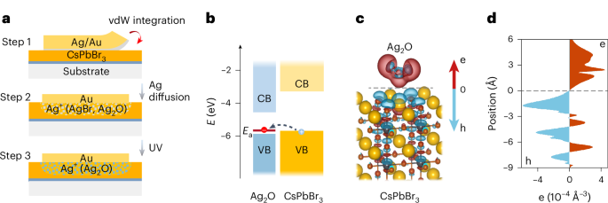
• Abstract Efficient carrier injection at metal-semiconductor interfaces is essential for probing intrinsic electronic properties and enabling high-performance devices. • Thinning the Schottky barrier via contact doping is a cornerstone strategy in semiconductor technology for minimizing contact resistance (Rc). • However, carrier doping in halide perovskites has remained elusive, and selective contact doping has not been achieved, resulting in excessive Rc that far exceeds the intrinsic material resistance. • Here we report an effective contact-doping strategy by transferring Ag/Au electrodes onto single-crystal CsPbBr3 thin films using a low-energy van der Waals integration process. • Moderate annealing (80-180 °C) during transfer enables silver diffusion into CsPbBr3, followed by its transformation into Ag2O clusters upon ultraviolet treatment, forming an Ag2O/CsPbBr3 bulk heterojunction. • The Ag2O clusters embedded in CsPbBr3 act as interfacial electron acceptors, inducing a local hole density of ∼5 × 1017 cm−3 in the contact region.
Article Summaries:
- Researchers have demonstrated a new contact‑doping technique for lead halide perovskites that dramatically lowers metal‑semiconductor contact resistance. By transferring Ag/Au electrodes onto single‑crystal CsPbBr₃ thin films using a low‑energy van der Waals integration process, moderate annealing (80-180 °C) allows silver to diffuse into the perovskite. Subsequent ultraviolet exposure converts the silver into Ag₂O clusters that embed within the crystal, forming a bulk heterojunction. These clusters act as interfacial electron acceptors, creating a local hole density of ~5 × 10¹⁷ cm⁻³ and shrinking the Schottky barrier. The approach reduces contact resistance to 26-70 Ω cm and yields a two‑terminal sheet conductance above 225 µS at 190 K, a significant improvement over conventional perovskite contacts.
- Abstract Efficient carrier injection at metal-semiconductor interfaces is essential for probing intrinsic electronic properties and enabling high-performance devices. Thinning the Schottky barrier via contact doping is a cornerstone strategy in semiconductor technology for minimizing contact resistance (Rc). However, carrier doping in halide perovskites has remained elusive, and selective contact doping has not been achieved, resulting in excessive Rc that far exceeds the intrinsic material resistance. Here we report an effective contact-doping strategy by transferring Ag/Au electrodes onto si
Sources:
- https://www.nature.com/articles/s41563-026-02485-x (Latest source article published: 2026-02-25 06:47 UTC)