• In the modern world, the semiconductor industry stands at the heart of technological innovation. • From smartphones and laptops to advanced medical devices and artificial intelligence systems, nearly every piece of contemporary electronics depends on increasingly sophisticated microchips. • Among the leading companies driving this progress is Taiwan Semiconductor Manufacturing Co., Ltd. • (TSMC), the world’s largest pure-play semiconductor foundry. • Through continuous research, advanced manufacturing techniques, and aggressive scaling strategies, TSMC has played a pivotal role in pushing the boundaries of what is possible in chip fabrication. • As semiconductor technology advances, one of the most critical goals is scaling down device dimensions.
Article Summaries:
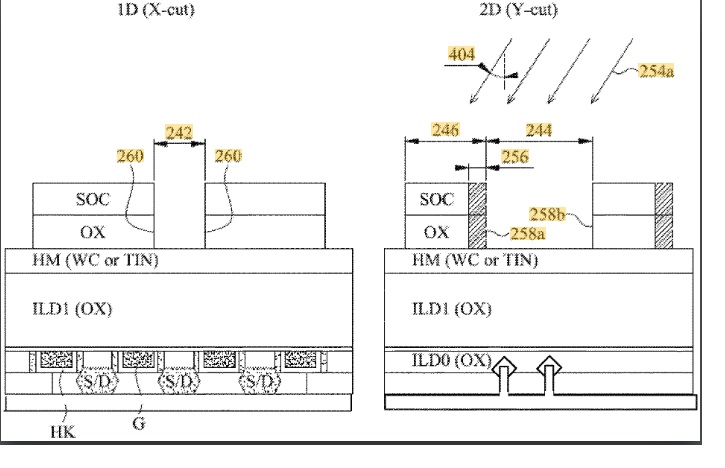
- TSMC has announced a new process simplification for its advanced 5 nm and smaller nodes that cuts lithography steps from three to one. The technique combines EUV lithography with a carefully engineered angled ion‑etch that trims or extends feature lengths without altering widths, enabling sub‑35 nm end‑to‑end spacing. By eliminating multiple pattern transfers, the method reduces cycle time, cost, and alignment errors while maintaining critical dimension control. The development is aimed at improving yield and reliability in high‑density chips, positioning TSMC to keep pace with the industry’s push toward ever smaller transistors.
Sources: