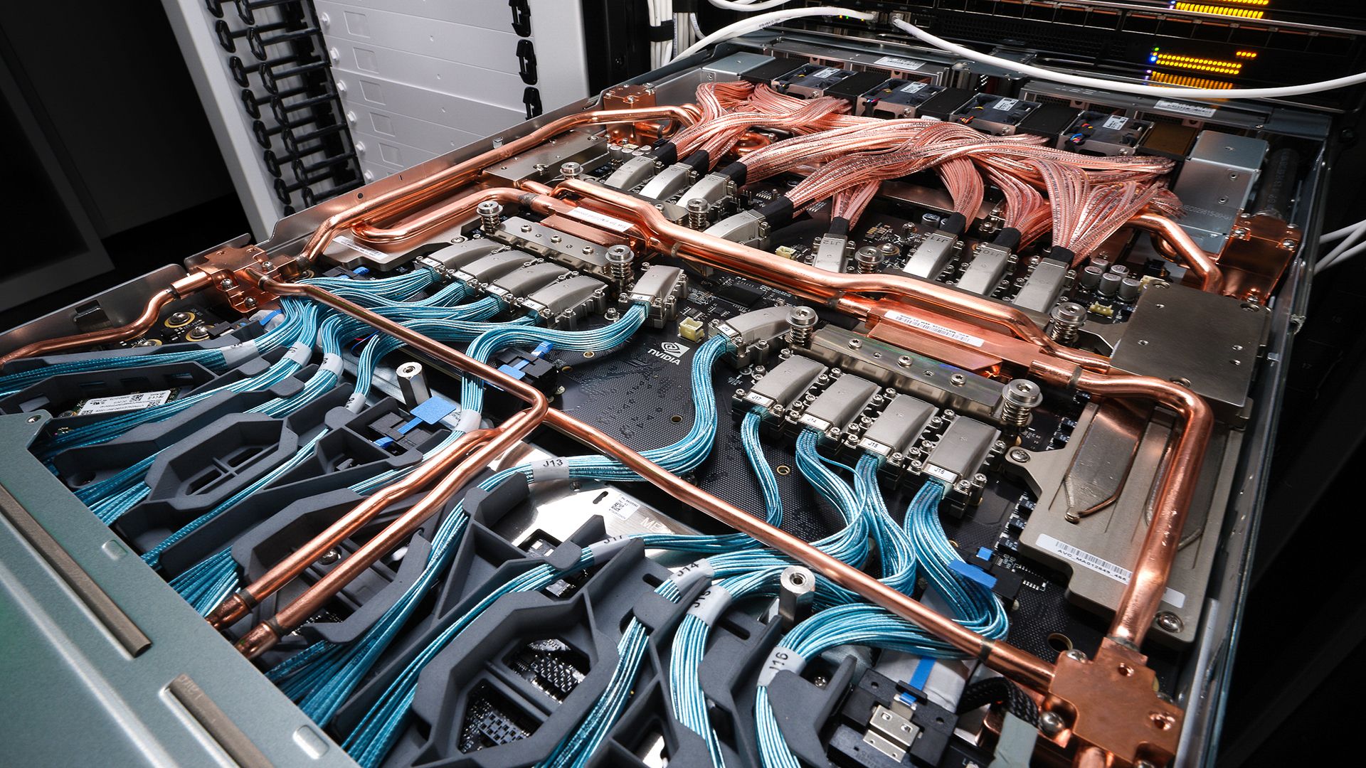
• UALink roadmap plots course to optimized AI data center interconnects - examining the open standard designed to combat vendor lock-in while offering cost and performance optimization Exploring the UALink standard, and its future. • Get Tom’s Hardware’s best news and in-depth reviews, straight to your inbox. • You are now subscribed Your newsletter sign-up was successful UALink (short for Ultra Accelerator Link) is an upcoming interconnect technology designed to enable high-speed, low-latency communication between AI accelerators (ASICs, GPUs, FPGAs, NPUs, XPUs) and other compute devices across a scale-up logical domain. • Many see it as an important path forward for the future of AI data centers due to its planned performance, cost, and power efficiency advantages, not to mention that, as an open standard, it will reduce vendor lock-in. • In 2025, the UALink Consortium published revision 1.0 of the UALink specification, marking a point after which hardware designers can officially implement the technology into their AI/HPC accelerators and switch ASICs required to build AI pods with up to 1,024 accelerators. • But while UALink technology is widely supported by the industry, and its specification that defines accelerator-to-accelerator comms is available now, its broad adoption is several years away.
Article Summaries:
- UALink, an open‑standard interconnect for AI accelerators, was formalised by the UALink Consortium with a 1.0 specification in 2025. The protocol supports up to 1,024 accelerators per pod, delivering 200 Gbps per lane (212.5 GT/s raw) and deterministic latency below 1 µs, with an effective bandwidth utilisation of about 93 %. Built on Ethernet‑PHY signalling and a lightweight layered stack, UALink aims to replace proprietary links such as Nvidia’s NVLink while reducing vendor lock‑in and cutting cost and power. Although widely backed by industry players, widespread deployment is expected several years out.
Sources: