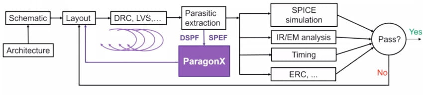
• IC layout parasitics dominate the performance of custom digital, analog and mixed-signal designs, so the challenge becomes how to identify the root causes and to quantify the effects of parasitics during early design stages. • The old method of iterating between layout, extraction, SPICE simulation, followed by manual debug and analysis is just too slow and error prone to be relied upon. • A smarter approach has been developed with an EDA tool calledParagonXfrom Synopsys, so I attended a recent webinar to become more informed. • ParagonX came from start-up Diakopto which was acquired by Ansys, then Synopsys acquired Ansys. • Rob Dohanyos of Synopsys opened up the webinar with an overview of ParagonX and then most of the time was spent in a live demo, something kind of rare with EDA vendors. • The ParagonX tool can be used by a circuit designer to analyze, debug, visualize and even optimize their IC layout parasitics for any technology node and any circuit design style.
Article Summaries:
- IC layout parasitics dominate the performance of custom digital, analog and mixed-signal designs, so the challenge becomes how to identify the root causes and to quantify the effects of parasitics during early design stages. The old method of iterating between layout, extraction, SPICE simulation, followed by manual debug and analysis is just too slow and error prone to be relied upon. A smarter approach has been developed with an EDA tool called ParagonX from Synopsys, so I attended a recent webinar to become more informed. ParagonX came from start-up Diakopto which was acquired by Ansys, the
- Synopsys’ new EDA tool, ParagonX, aims to accelerate IC layout parasitic analysis by replacing the slow, manual cycle of layout, extraction, SPICE simulation, and debugging. Developed from the start‑up Diakopto (now part of Ansys, then Synopsys), ParagonX lets designers load large netlists (hundreds of GB) and analyze millions of nodes quickly through a binary database and interactive GUI. The tool offers point‑to‑point resistance, sensitivity mapping, capacitive coupling, and RC‑delay calculations, all scriptable in Python. In a recent webinar, a live demo showed how the tool can cut parasitic debugging time from weeks to minutes, benefiting high‑speed, high‑precision, and analog designs down to 3 nm nodes.
Sources: