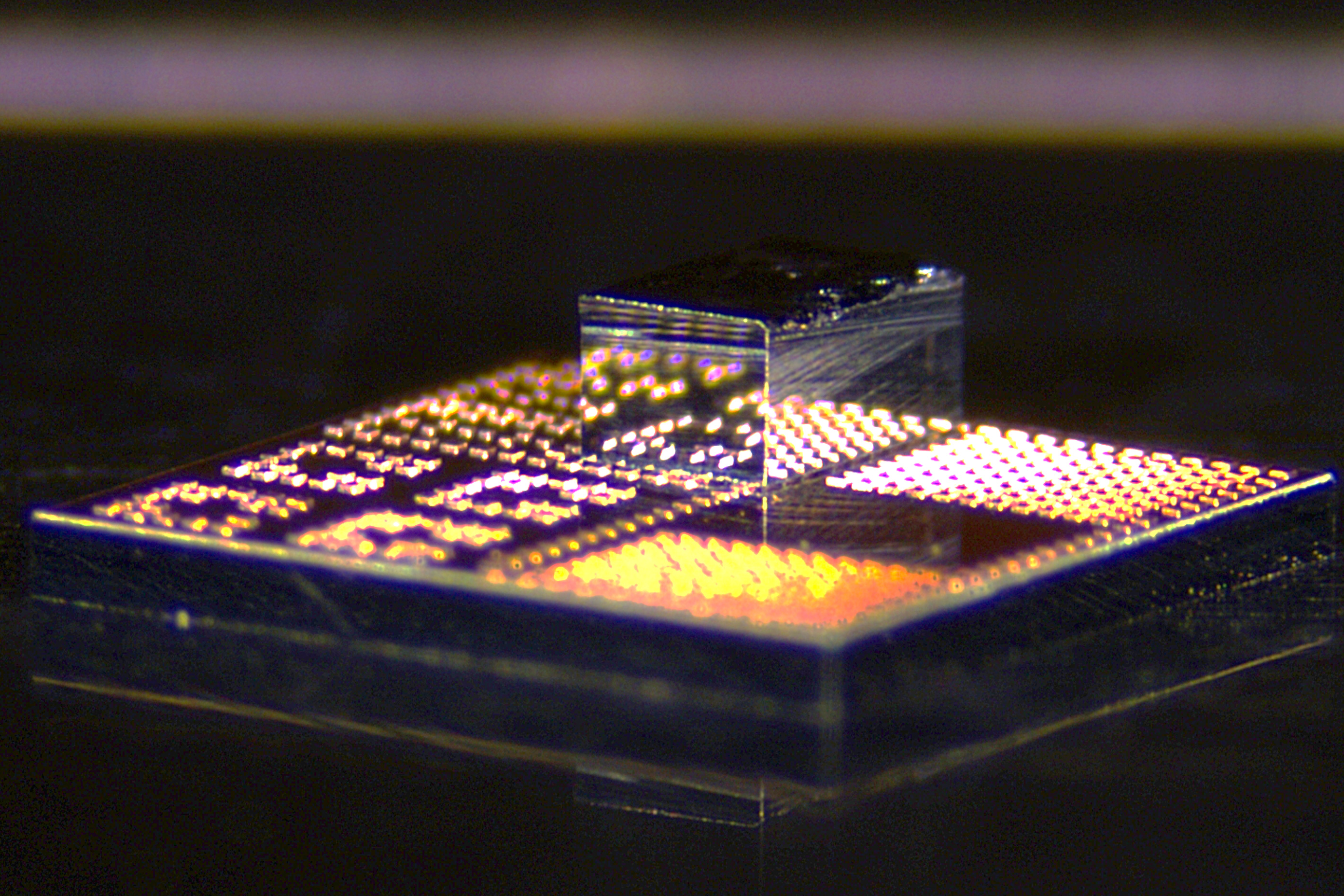
• Breadcrumb MIT News New 3D chips could make electronics faster and more energy-efficient New 3D chips could make electronics faster and more energy-efficient Press Contact: Media Download *Terms of Use: Images for download on the MIT News office website are made available to non-commercial entities, press and the general public under aCreative Commons Attribution Non-Commercial No Derivatives license. • You may not alter the images provided, other than to crop them to size. • A credit line must be used when reproducing images; if one is not provided below, credit the images to “MIT.” Previous imageNext image Audio The advanced semiconductor material gallium nitride will likely be key for the next generation of high-speed communication systems and the power electronics needed for state-of-the-art data centers. • Unfortunately, the high cost of gallium nitride (GaN) and the specialization required to incorporate this semiconductor material into conventional electronics have limited its use in commercial applications. • Now, researchers from MIT and elsewhere have developed a new fabrication process that integrates high-performance GaN transistors onto standard silicon CMOS chips in a way that is low-cost and scalable, and compatible with existing semiconductor foundries. • Their method involves building many tiny transistors on the surface of a GaN chip, cutting out each individual transistor, and then bonding just the necessary number of transistors onto a silicon chip using a low-temperature process that preserves the functionality of both materials.
Article Summaries:
- MIT researchers have devised a low‑cost, scalable method to integrate gallium nitride (GaN) transistors onto standard silicon CMOS chips. The process cuts individual high‑performance GaN transistors from a GaN wafer, then bonds only the needed units onto a silicon chip using a low‑temperature technique that preserves both materials’ functionality. The resulting hybrid chips deliver significant speed and power‑efficiency gains while keeping GaN usage minimal, thereby reducing cost and system temperature. A proof‑of‑concept power amplifier for mobile phones achieved higher signal strength and efficiency, promising better call quality, bandwidth, and battery life. The technique is compatible with existing foundries and could extend to quantum computing applications.
Sources: