• Copy link Facebook X Whatsapp Reddit Pinterest Flipboard Email Get Tom’s Hardware’s best news and in-depth reviews, straight to your inbox. • You are now subscribed Your newsletter sign-up was successful ASML this week reaffirmed that it is on track to release a Twinscan NXE extreme ultraviolet lithography system that features a 1000W EUV power source and can process up to 330 wafers per hour. • The system, projected for sometime in 2030 or beyond, offers 50% more power than the current best EUV tool, the NXE:3800E. • Such machines will greatly decrease productivity and decrease costs per wafer for chipmakers, but to make them possible, ASML has had to achieve several breakthroughs. • A deeper look at the chipmaking supply chain TSMC’s $165 billion U.S. • investments examined China reportedly reverse-engineers EUV tool China bets on DUV, as EUV blockade reshapes chipmaking “What was achieved - one kilowatt - is pretty amazing,” Michael Purvis, ASML’s lead technologist for its EUV source light, toldReuters.
Article Summaries:
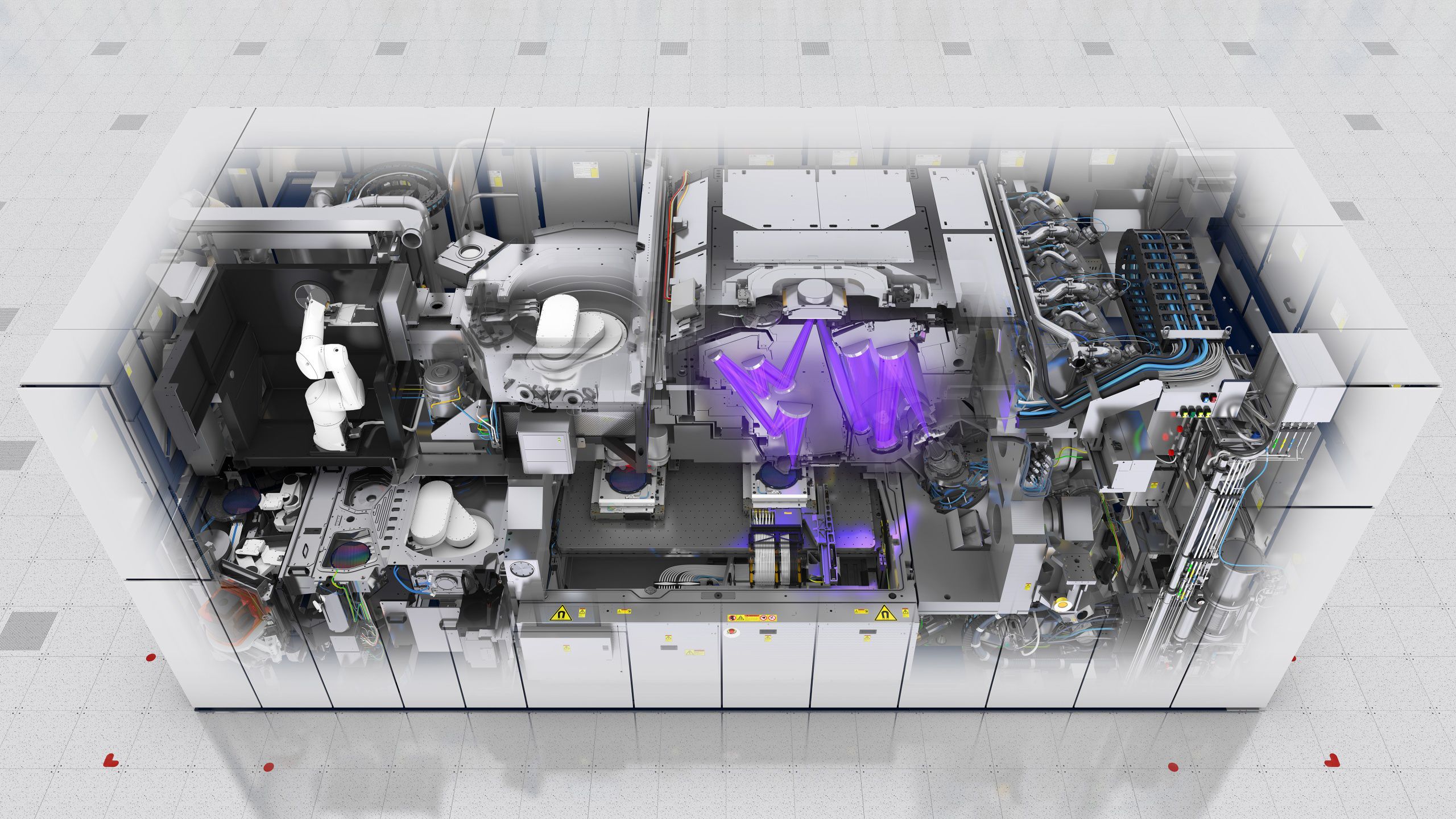
- ASML announced that its upcoming Twinscan NXE EUV lithography system will feature a 1,000‑watt light source and can process up to 330 wafers per hour, a 50 % power increase over the current NXE:3800E. The breakthrough relies on doubling tin droplet production to 100,000 per second and adding a second laser pulse sequence, enabling the higher EUV output. To manage the increased debris and transmission demands, ASML has developed new debris collectors, high‑transmission optics, and will require updated resists and pellicles. The 1,000‑W system is slated for release around 2030, supporting ASML’s roadmap to higher productivity and lower wafer costs.
- ASML announced that its upcoming Twinscan NXE extreme‑ultraviolet (EUV) lithography system will feature a 1,000‑watt EUV source and can process up to 330 wafers per hour, a 50 % power increase over the current NXE:3800E. The new light source relies on a three‑pulse generation scheme-two 1 µm pre‑pulses to shape tin droplets and a 10 µm CO₂ main pulse to produce EUV plasma-along with a tin‑droplet injector that will double the droplet rate to 100,000 per second. To handle the higher debris load and transmission demands, ASML is developing new debris collectors, high‑transmission projection optics, and upgraded stages, while the semiconductor industry prepares new resists and pellicles for the next‑generation tools.
Sources: