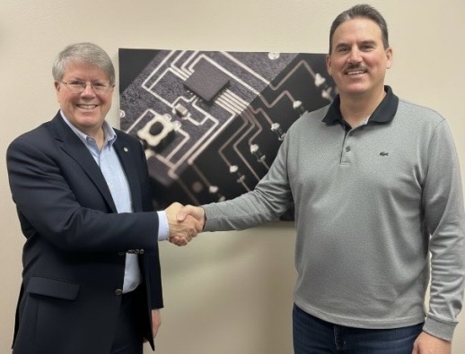
• APES Partners with Great Lakes Semiconductor to Scale Advanced, Additive Chip Packaging Share this Article Terminologically, additively manufactured electronics (AME) occupies similar space in the realm of tiny components that additive construction (AC) occupies when it comes to large components: it’s a single phrase that in fact refers to a kaleidoscope of applications that continues to constantly diversify. • The same way that AC covers a range of use-cases, fromWal-Mart warehousesandsubsurface structurestoself-sufficient farmhouses, AME subsumes everything fromRF antennasto rapidly iterated PCB prototypes. • While it might not get the same level of attention as use-cases like next-gen wearables,advanced chip packagingmay ultimately prove to represent the most singular growth opportunity for the AME market segment. • In that sense,Advanced Printed Electronics Solutions(APES) of New York is the future of electronics 3D printing. • That future just got pulled a little closer to the present with APES’ announcement that the company has partnered withGreat Lakes Semiconductor(GLS) to incorporate the APES Matrix6D platform into the GLS Fab-as-a-Service (FaaS) model. • APES unveiledits Matrix6D platformat last year’s RAPID + TCT show, and 3DPrint.com’s Joris Peels described it like this: “The Matrix6D is a modular 3D printing solution featuring movable maglev conveyor platforms that travel beneath various print heads.
Article Summaries:
- Terminologically, additively manufactured electronics (AME) occupies similar space in the realm of tiny components that additive construction (AC) occupies when it comes to large components: it’s a single phrase that in fact refers to a kaleidoscope of applications that continues to constantly diversify. The same way that AC covers a range of use-cases, from Wal-Mart warehouses and subsurface structures to self-sufficient farmhouses, AME subsumes everything from RF antennas to rapidly iterated PCB prototypes. While it might not get the same level of attention as use-cases like next-gen wearabl
Sources:
- https://3dprint.com/324179/apes-great-lakes-semiconductor-to-scale-advanced-additive-chip-packaging/ (Latest source article published: 2026-02-24 14:00 UTC)